Ultra-fine spherical silica filler designed for high-frequency and
high-speed electronic materials, improving dimensional stability
and signal transmission performance.
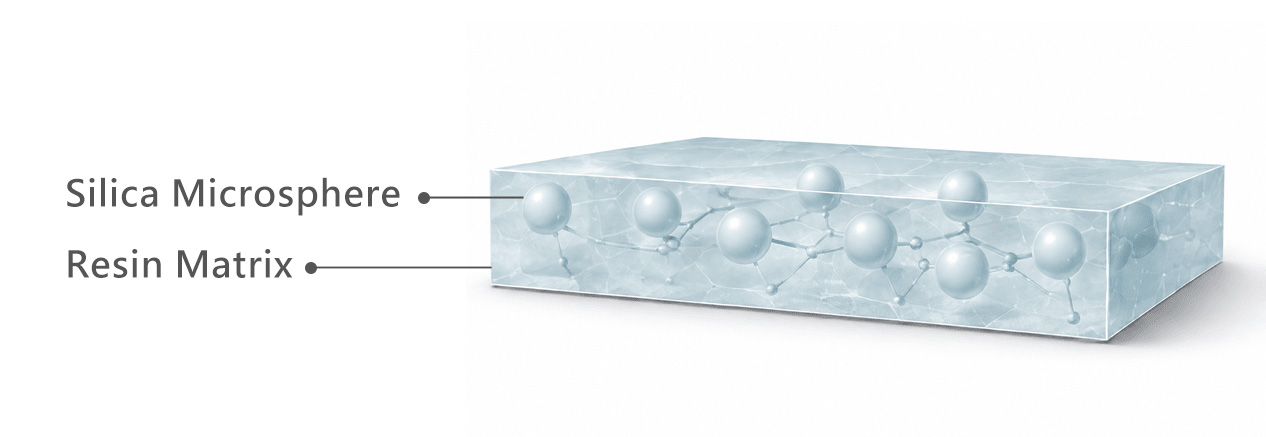
Entire Technology's Low Dk/Df Microsphere Silica Filler is
engineered for Copper Clad Laminate and IC substrate applications.
Its excellent thermal stability helps minimize the thermal
expansion of resin substrates, improving compatibility with copper
foil and semiconductor chips and enhancing dimensional stability
during high-temperature processing. Its ultra-low dielectric
properties also help reduce signal loss and propagation delay,
supporting stable high-frequency and high-speed signal
transmission.
- Features & Benefits -
Low CTE
Reduces substrate thermal expansion to better match copper foil
and chips, helping minimize warpage or delamination during
high-temperature processing.
High Sphericity
High sphericity provides excellent flowability, helping optimize
filler loading while reducing drilling tool wear.
Low Df
Reduces energy dissipation along high-frequency signal
transmission paths to maintain signal integrity.
Low Dk
Helps reduce signal distortion and propagation delay in
high-frequency applications.
High Dimensional Stability
Maintains structural stability under high-temperature and
high-pressure processing conditions.
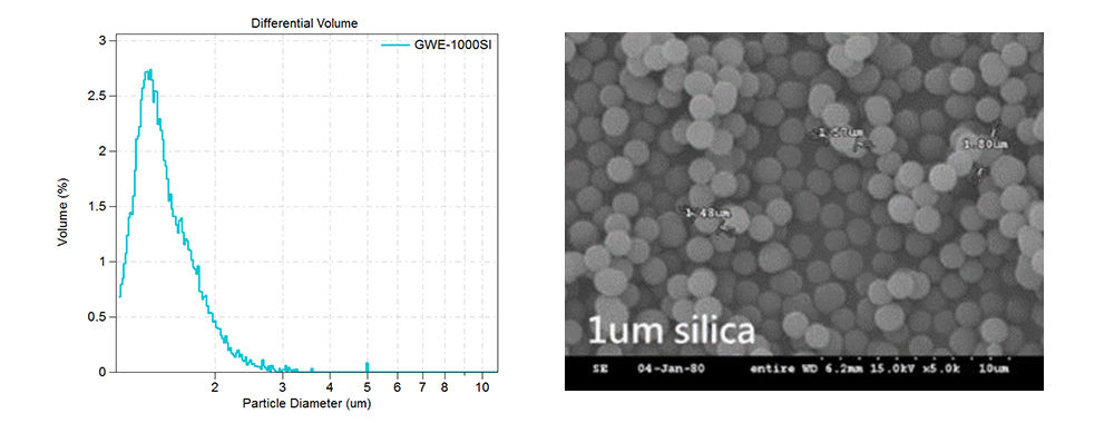
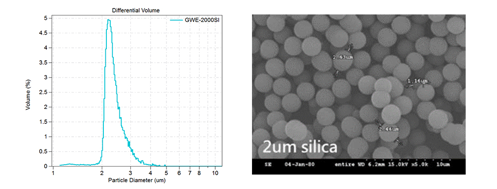
- Technical Evidence -
Particle size distribution and microstructure characterization
demonstrate the particle size and spherical morphology of the silica
filler.
- Applications -
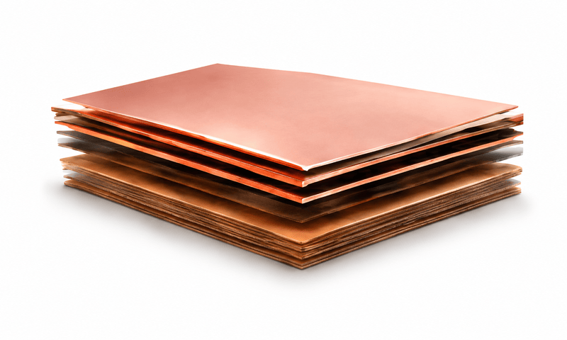
Copper Clad Laminate (CCL)
Suitable for high-frequency and high-speed electronic
material applications, supporting dimensional stability and
reliable signal transmission.
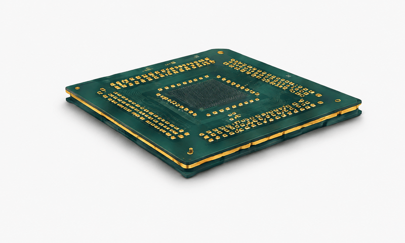
IC Substrate
Excellent thermal stability and low dielectric properties
support demanding high-end IC substrate applications.
For samples, technical information, or business inquiries,
please contact us.
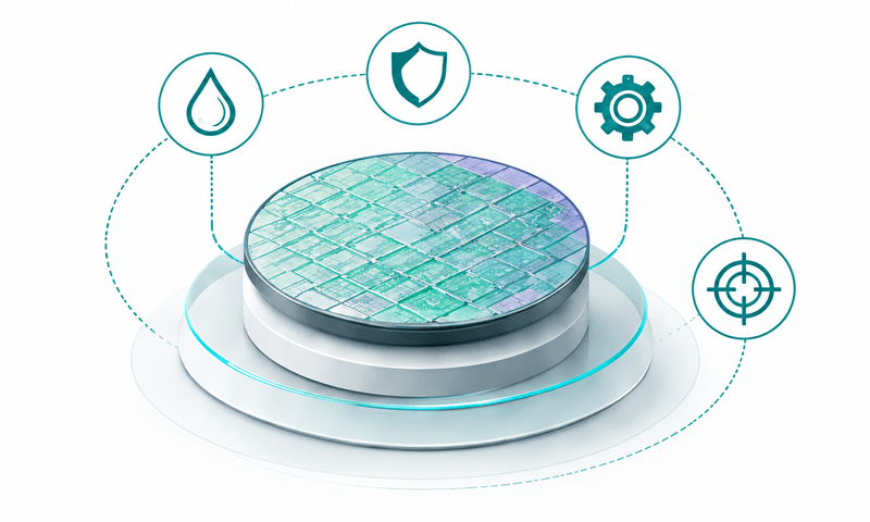
Designed for semiconductor processes such as wafer thinning,
dicing, and die pickup, our high-performance base film solutions
deliver process protection, stable handling, and clean release
performance.
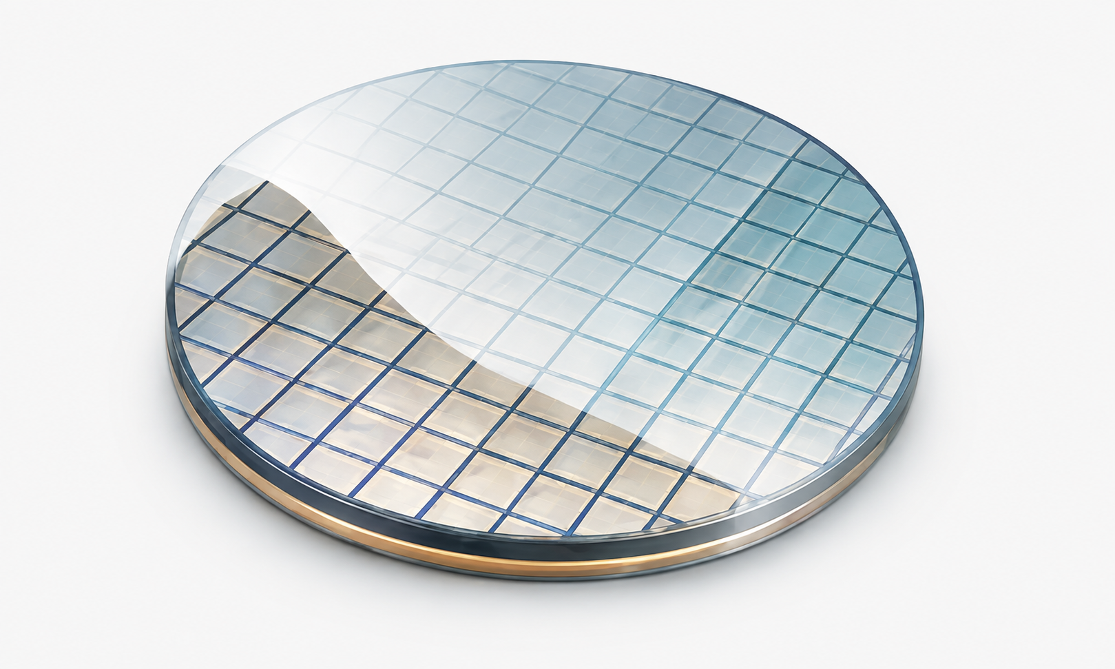
Entire Technology's semiconductor process films are engineered for
critical processes including wafer back grinding, dicing,
expansion, and die pickup. With excellent mechanical buffering,
process stability, and clean debonding performance, these film
solutions help improve process reliability and yield while meeting
the precision requirements of advanced semiconductor
manufacturing.
High Cleanliness & Low Residue
Mechanical Performance & Stretchability
Process Stability & Yield Improvement
Material Platform
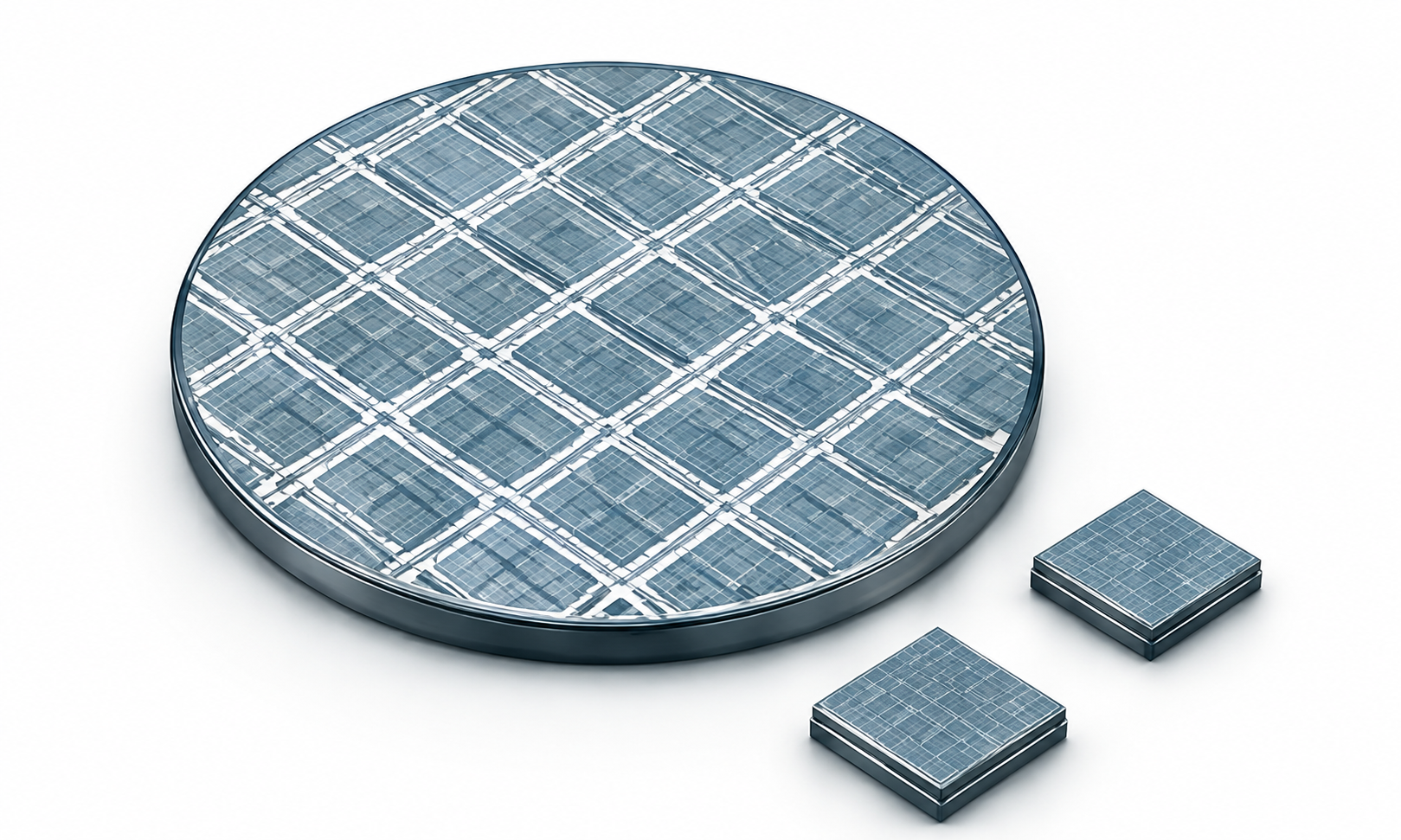
Semiconductor Process Flow
Wafer
→
B/G Tape Base Film
Back Grinding
Wafer Surface Protection、Stress Absorption、Grinding
Thickness Control
→
Dicing Tape Base Film
Dicing
→
Expansion
→
Die Pickup
Die Fixation、Water-Resistant Dicing、Uniform Expansion、Die
Pickup
B/G Tape Base Film Back Grinding Tape Base Film
Designed for wafer back grinding processes, the B/G Tape Base
Film provides excellent thickness uniformity, step coverage,
and mechanical buffering to protect delicate wafer
microstructures and support stable wafer thinning performance.
Low Total Thickness Variation
Optimizes wafer thickness uniformity and helps reduce
warpage and cracking after thinning.
High Step Coverage
Provides effective coverage over fine wafer structures to
help prevent process fluid penetration.
Advanced Mechanical Buffering
Absorbs mechanical stress generated during wafer thinning to
protect delicate wafer microstructures.
Residue-Free Interfacial Delamination
Enables controlled adhesion reduction after UV irradiation
for clean and efficient debonding.
Dicing Tape Base Film
Designed for wafer dicing, expansion, and die pickup
processes, the Dicing Tape Base Film provides excellent shear
strength and water resistance for secure die fixation during
dicing, together with biaxial stretchability and UV-controlled
adhesion reduction for efficient downstream processing.
High Shear Strength
Securely holds individual dies and helps prevent die shift
during wafer dicing.
Superior Water Resistance
Maintains stable adhesion and helps prevent water ingress
during dicing and high-pressure rinsing.
Excellent Biaxial Stretchability
Provides uniform biaxial expansion to facilitate die
separation while reducing tape tearing risk.
Precision UV-Curable Technology
Provides stable adhesion during dicing and controlled
adhesion reduction after UV irradiation for efficient die
pickup.
- Core Technical Capabilities -
Process Stability
Consistent and reliable performance across different process
conditions.
Wafer Protection
Mechanical buffering helps reduce wafer damage risk during
grinding and dicing.
Precision Interface Control
Precisely controlled adhesion and release behavior for different
semiconductor processes.
Yield Improvement
Integrates material and process performance to support overall
yield and reliability.
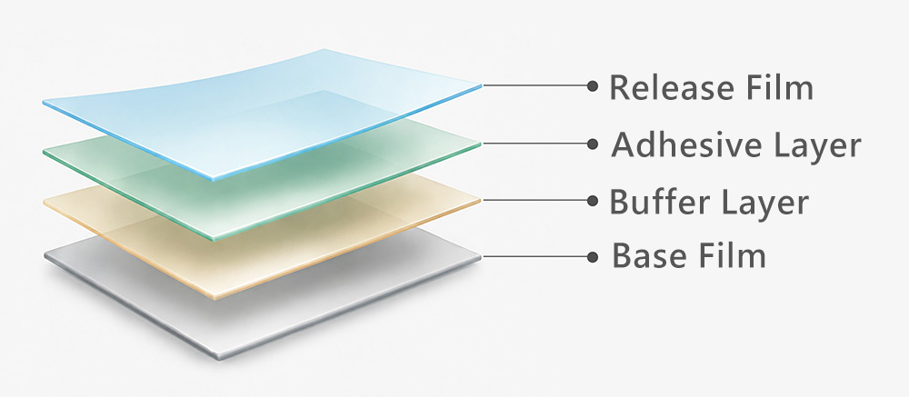
- Film Structure -
Material Platform
PVC / PO / EVA / PET
Release Technology
UV-Controlled Debonding
Customized Design
Film structure and properties can be adjusted based on process
and application requirements.
- Applications -
Back Grinding
Wafer Dicing
Wafer Expansion
Die Pickup
Semiconductor Packaging
Need a customized semiconductor process film solution?
Contact Entire Technology to discuss film solutions tailored to
your process and application requirements.
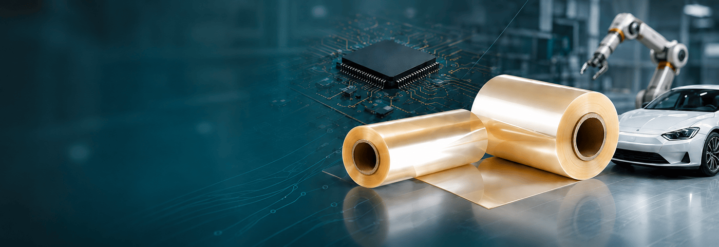
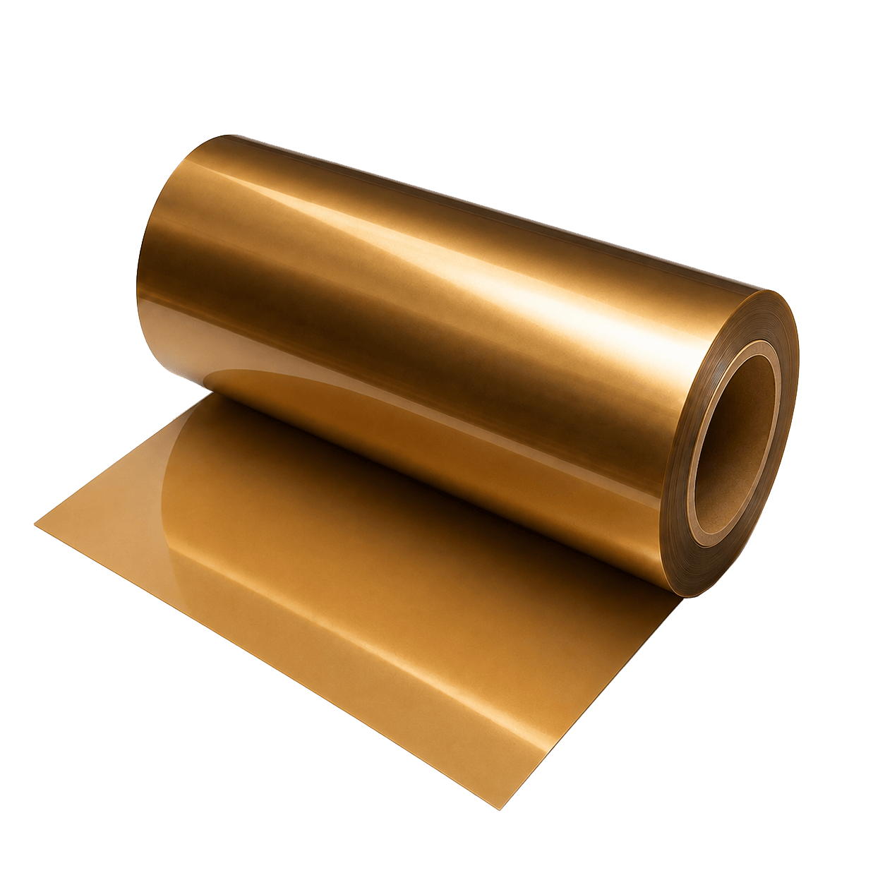
Designed for semiconductor, electronics, automotive and advanced
industrial applications, our high-temperature insulating films
deliver excellent heat resistance, electrical insulation, chemical
resistance and dimensional stability.
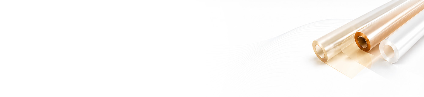
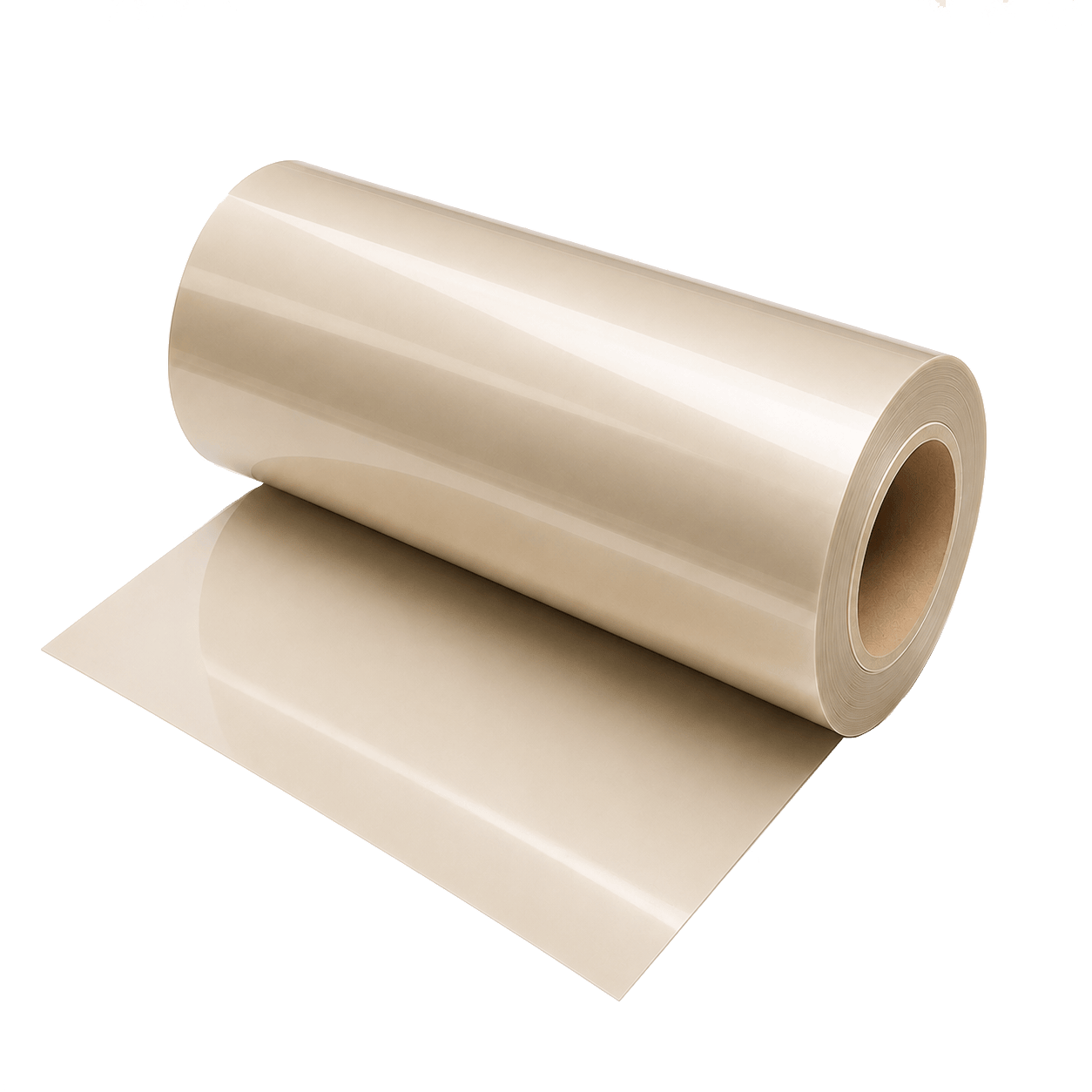
Entire high-temperature insulating films are developed for
high-temperature processes and demanding environments. We provide
a variety of material, thickness and functional solutions to meet
customer design, processing and application needs.
- Key Performance -
Excellent Heat Resistance
Maintains stable performance under prolonged high-temperature conditions.
Excellent Electrical Insulation
Superior insulation performance ensures electrical safety.
Chemical Resistance
Excellent resistance to chemicals for extended service life.
Dimensional Stability
Low thermal expansion ensures dimensional stability and minimizes deformation.
Mechanical Strength & Wear Resistance
High mechanical strength and wear resistance for enhanced reliability.
Customizable Solutions
Materials, thickness, and functionality can be customized to meet specific requirements.
- Applications -
Semiconductor Process
Process protection, electrical insulation and high-temperature
film materials for semiconductor manufacturing.
Flexible Circuit Board
Suitable for FPCB, rigid-flex boards and heat-resistant
insulation applications.
Electronics & Electrical
Used for motor insulation, sensors, electronic components and
protective materials.
Automotive & Aerospace
Designed for high-temperature insulation, lightweight structures
and high-reliability applications.
Consumer Electronics
Suitable for acoustic diaphragms, wearable devices and precision
electronic components.
Industrial Equipment
Provides chemical resistance, wear resistance and protection in
high-temperature environments.
- Material Solutions -
PEEK Series Film
High heat resistance, chemical resistance and wear
resistance
Good mechanical strength and fatigue resistance
Suitable for electronic insulation, industrial and aerospace
applications
TPI Series Film
High heat resistance with thermoplastic processability
Excellent electrical insulation and chemical resistance
Suitable for FPCB, semiconductor and high-temperature
insulation applications
Other Customized Materials
In addition to the above materials, other high-temperature
insulating films can be evaluated and developed based on
customer application conditions, processing temperature,
thickness and functional requirements.
- Material Selection Guide -
Evaluation Items
PEEK Series
TPI Series
Remarks
Heat Resistance
★★★★★
★★★★★
Varies depending on material type and thickness
Electrical Insulation
★★★☆☆
★★★★★
Varies depending on material type and thickness
Chemical Resistance
★★★★★
★★★★☆
Varies depending on the actual chemical environment
Mechanical & Wear Resistance
★★★★★
★★★☆☆
Varies depending on processing and operating conditions
Thermoplastic Processability
★★★☆☆
★★★☆☆
Varies depending on processing equipment and conditions
Typical Applications
Electronics, Acoustics, Machinery, Aerospace
FPCB, Semiconductor, Electrical Insulation
—
Rating Guide:★★★★★Excellent/★★★★☆Good to Excellent/★★★☆☆Good